Wafer Optical Inspection Solution for Semiconductor Front-End Manufacturing
26.03.2020
Background
During semiconductor front-end manufacturing, the CMP(chemical mechanical planarization) process of smoothing surfaces with a combination of chemical and mechanical forces sometimes results in surface damage like cracks and scratch defects. Effectively addressing this risk requires anon-destructive, non-contact, wave-length sensitive vision inspection for surface purity and planarity. Advantech offers a machine vision total solution covering industrial-grade image sensors, high-level computing,multiple core processor, and the VisionNavi application software—a user-friendly, flowchart-based interface that can simplify development and deployment, branch and loop functions for advanced vision applications, and support multiple tasks and cameras with a global shutter to deliver precise and efficient semiconductor production.
System Requirements
The customer is a leading wafer manufacturing company in the semiconductor industry who required an inspection system that could locate damage and defects during the CMP process. Due to the characteristic materials of the wafers, a non-destructive, non-contact,wave-length sensitive vision inspection for surface purity and planarity was essential. The vision inspection system needed to be synchronized with the automated robotic handling system in order to increase productivity. The goal of inline vision inspection equipment was to provide high-precision analysis while maintaining productivity levels. The customer was looking for a complete system capable of performing at speed, with highly accurate inline inspection. The customer also wanted to reduce installation/maintenance effort, since there were many different kinds of wafers and defect types.
System Description
Advantech’s machine vision edge solution was installed as the CMP system. The system included CMP machinery, robotic handling system, a vision inspection system, and uplink data for the IT database.After the wafers were polished, the position sensor sent a triggering signal to the vision system. Multiple images from different camera angles were acquired and sent to the vision system, where VisionNavi software processed the images for defect inspection, then verified the wafers. The vision system sent out an “NG” signal to reject a wafer if a defect was detected oran “OK” signal to pick up the wafer for the next process. Image data was restored and integrated with the customer’s current enterprise databases.
System Architecture
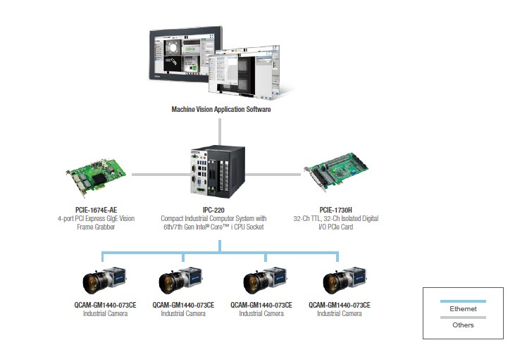
Solution Components
-
IPC-220: Compact IndustrialComputer System with6th/7th Gen Intel® Core™i CPU Socket
-
PCIE-1674E-AE: 4-port PCI Express GlgEVision Frame Grabber
-
PCIE-1730H: 32-Ch TTL, 32-ChIsolated DigitalI/O PCIe Card
-
QCAM-GM1440-073CE: Industrial Camera
Why Advantech?
Advantech’s Machine Vision Inspection System integrates the global shutter, high speed industrial cameras, a multi-channelcomputing platform, and vision software, so that users don’t need to worry about how to select compatible products.The VisionNavi software is designed with a graphical and flowchart-based interface, where users can easily complete thedevelopment and deployment of vision inspection applications without any programming skills.
For further information:
IPC-220/240: https://www.advantech.com/campaign/compact-ipc
/PCIE-1761H_3D _S20181009184206.jpg)
/PCIE-1754_S20120815175551.jpg)
/PCI-1750_B20160905135030.png)
/PCIE-1758DI0_3D _S20181220172640.jpg)